
Inovation
Facing the Future: Europe’s Next Big Test
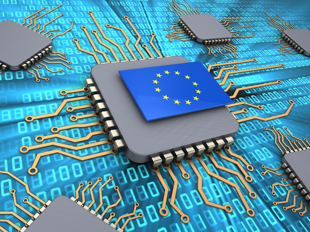
The European Chips Act is a strategic response by the European Union to the challenges and opportunities in the semiconductor sector, aiming to increase Europe’s market share from 10% to 20% by 2030 through a planned investment of over €43bn.
This groundbreaking initiative recognizes the importance of semiconductors in various technologies, from smart devices to electric vehicles, as society becomes more technology-dependent. The EU’s strategic plan focuses on Pilot Lines, dedicated facilities for innovation and streamlined production of cutting-edge semiconductor technologies.
The EU Chips Act addresses the need for strategic autonomy and the green and digital twin transition. This transition involves digitalization and sustainability to combat climate change. The semiconductor industry is crucial in driving these transitions through its enabling technologies.
Two main consequences of the twin transition are the electrification of industries and transport, shifting away from carbon-rich energy sources, and the rapid increase in connectivity and data volumes. The semiconductor industry, particularly in power chip development, plays a key role in meeting these demands.
Wide bandgap (WBG) materials like silicon carbide (SiC) and gallium nitride (GaN) are replacing conventional silicon in power chips. These materials offer higher voltages, faster switching speeds, and efficient power conversion, making them ideal for applications in digital and green transitions.
The European semiconductor industry excels in WBG materials, driving advancements in automotive, industrial, and telecommunication sectors. Companies like Infineon, ST, and NXP lead the market and contribute to digitalization and electrification.
The WBG materials have gained traction for power electronics and telecommunications, transitioning from a commodity market to more innovative solutions. Manufacturing processes and architecture developments are ongoing to improve energy efficiency and reduce costs.
The WBG pilot line project aims to expand the European semiconductor industry’s competitiveness by enabling the adoption of advanced WBG technologies in high-value applications. This distributed facility across Europe will drive innovation and collaboration in materials and device development.
The pilot line will focus on developing advanced processes for materials growth and device fabrication, with a high level of automation and yield. It will also explore new materials like AlN and Ga2O3 for next-generation semiconductors.
Through the WBG pilot line, the European semiconductor industry aims to revolutionize testing and experimentation of advanced technologies, introducing new materials and devices to address societal challenges in energy efficiency and sustainability.
Overall, the WBG pilot line project will have a significant impact on the development of novel technological approaches in semiconductors, accelerating the transition to more efficient and sustainable electrical systems for various market sectors.


Avatar Legends: The Fighting Game – Secure Your Copy Now!

Fitbit Air: The Golden Opportunity for Google’s Next Big Move

Even Realities Secures $150M Funding from Meituan and Tencent, Reaches $1B Valuation in Smart Glasses Industry

Ultimate Guide to Camera Phones, Android Security, and Data Privacy: Everything You Need to Know in August 2026

Comparing Five BMW X5 Powertrains: Unveiling the Differences

“Fortify and Defend: Construct a Medieval Castle and Battle Enemy Knights in Bergfried” This title highlights the strategic gameplay of building and defending a castle piece by piece, as well as the intense battles against enemy knights in the city builder and real-time strategy game Bergfried. Players will experience the thrill of constructing a formidable fortress and strategically defending it against relentless enemies in this immersive medieval simulation.

Battle of the Slim Power Banks: Xiaomi UltraThin Magnetic Power Bank 5000 vs Ugreen MagFlow Air 5K

Boost Your Tender Win Rates by up to 50% with BidScript: Secures €701k Pre-Seed Funding

Samsung S10 Plus vs iPhone XS Max / Mate 20 Pro EXTREME Camera Test

EU Takes Action Against Instagram and Facebook for Violating Illegal Content Rules

Warning: Facebook Creators Face Monetization Loss for Stealing and Reposting Videos

Facebook’s New Look: A Blend of Instagram’s Style
Facebook Compliance: ICE-tracking Page Removed After US Government Intervention

Facebook and Instagram to Reduce Personalized Ads for European Users

InstaDub: Meta’s AI Translation Tool for Instagram Videos

Reclaim Your Account: Facebook and Instagram Launch New Hub for Account Recovery

Meta discontinues Messenger apps for Windows and macOS

Breaking Updates: Meta Connect 2025 Unveils Latest Developments
Samsung S10 Plus vs iPhone XS Max / Mate 20 Pro EXTREME Camera Test

This Smartphone lasts 50 DAYS without Charging.

Samsung S10 Plus Review – 6 things I love – 2 I hate.

Samsung S10 Plus vs iPhone XS Max / Mate 20 Pro – Speed Test!

The BEHEMOTH flagship smartphone for $230?

I just found out how much Google knows about me…

Mrwhosetheboss – Draw My Life – V2

12 Smartphone Gadgets you might not believe Existed.

Nokia 9 PureView – THIS is what FIVE Cameras can do.
-
 Facebook8 months ago
EU Takes Action Against Instagram and Facebook for Violating Illegal Content Rules
-
 Facebook9 months ago
Warning: Facebook Creators Face Monetization Loss for Stealing and Reposting Videos
-
 Facebook7 months ago
Facebook’s New Look: A Blend of Instagram’s Style
-

 Facebook9 months ago
Facebook Compliance: ICE-tracking Page Removed After US Government Intervention
-
 Facebook7 months ago
Facebook and Instagram to Reduce Personalized Ads for European Users
-
 Facebook9 months ago
InstaDub: Meta’s AI Translation Tool for Instagram Videos
-
 Facebook7 months ago
Reclaim Your Account: Facebook and Instagram Launch New Hub for Account Recovery
-
 Apple9 months ago
Meta discontinues Messenger apps for Windows and macOS